IUP Council of Trustees Approve Academic Affairs Committee Recommendations
On Wednesday, June 25, the Indiana University of Pennsylvania Council of Trustees approved recommendations from the Academic Affairs Committee,...

On Wednesday, June 25, the Indiana University of Pennsylvania Council of Trustees approved recommendations from the Academic Affairs Committee,...

Thomas R. Smith, an Indiana University of Pennsylvania graduate who had an almost 40-year career in education and supporting high school students,...

IUP Vice President for Student Affairs Thomas C. Segar was an invited presenter for a national conference sponsored by the Historically Black...

On June 16, Indiana University of Pennsylvania and Chan Soon-Shiong Medical Center at Windber formalized a clinical training affiliation agreement...

Indiana University of Pennsylvania has been selected by the Department of Defense POW/MIA Accounting Agency through the Henry M. Jackson Foundation...

Larry and Barb Kubala, of Indiana, graduates of Indiana University of Pennsylvania, are continuing their support of IUP with a gift of $25,000 to...

Indiana University of Pennsylvania hosted 22 area high school students and 14 of their teachers for the collaborative Healthcare Education and...

Indiana University of Pennsylvania and Indiana Regional Medical Center’s (IRMC) joint podcast, Rural Health Pulse, continues its third season...

Miko Rose, the founding dean of Indiana University of Pennsylvania’s proposed college of osteopathic medicine, will be a panelist during the...

Dean’s List recipients for the spring 2025 semester at Indiana University of Pennsylvania.

Dennis Popovec, a 1977 business and accounting graduate of Indiana University of Pennsylvania, originally from Westmoreland County, has continued...

On May 21, Indiana University of Pennsylvania and Conemaugh Meyersdale Medical Center formalized a clinical training affiliation agreement for...

Indiana State Normal School opened on May 17, 1875, beginning the journey IUP continues today, 150 years later. Watch the video IUP 150: A Legacy...

If they are valued so much as keepsakes and historical records, why did IUP yearbooks go away?

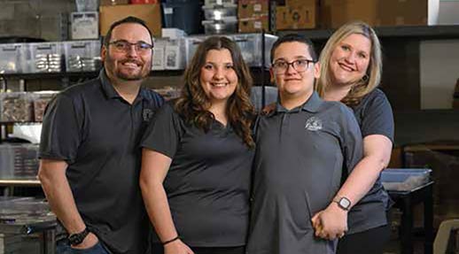
Find out why Roger Haney left hospital administration to get into the chocolate business.

A collaboration between IUP and the Center for Rural Pennsylvania on a study, “Understanding Physician Retention in Rural...

After more than three years in Russian confinement, Marc Fogel is back in the US.

As the first Crimson Scholar to graduate, Victoria Alao leads the way for others who have benefited from the program’s support.

See what the university has planned for this special anniversary.

Nearly 1,500 new graduates were honored during three commencement ceremonies on Saturday, May 10, at the Kovalchick Complex. Experience Spring 2025...

Indiana University of Pennsylvania and Indiana Regional Medical Center’s (IRMC) joint podcast, Rural Health Pulse, continues its third season...

An Indiana University of Pennsylvania alumni couple from Mechanicsburg who had life-long careers in education has established a scholarship for IUP...

On May 8, Indiana University of Pennsylvania’s Council of Trustees presented a resolution of appreciation to Jerry Pickering for his 25 years...

On May 8, members of Indiana University of Pennsylvania’s Council of Trustees heard a presentation about a new dual enrollment program...

On May 8, Indiana University of Pennsylvania’s Council of Trustees honored Shagufta Haque for her service on the Council with a resolution of...